
Introduction
When engineers discuss dry film photoresist for printed circuit board manufacturing, attention usually goes first to the photosensitive resin.
However, another material plays a critical supporting role throughout coating, handling and exposure:
the PET base film.
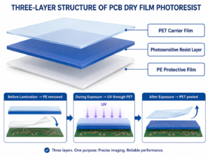
In dry film resist systems, a photosensitive resin layer is laminated onto a light-transmitting polyester base film, while a polyethylene cover film is typically used on the opposite side for protection. During PCB processing, the cover film is removed, the photosensitive layer is laminated onto the circuit-board substrate, and UV exposure is carried out through the PET base film before the carrier is peeled away for subsequent development. This general construction and process are described in Toray’s polyester-film patent for dry photoresist applications.
KOLON Industries likewise describes dry film as a film-type material used to form circuits and patterns in printed circuit boards and related electronic applications.
This means PET base film is not simply packaging for the photoresist.
Its optical quality, surface condition, thickness consistency, cleanliness, mechanical behavior and peel characteristics can all influence how reliably the dry film performs during PCB imaging.
As PCB wiring becomes finer, these film properties become increasingly important. Toray specifically identifies miniaturization of circuit-board wiring as a driver for advanced dry-film-resist PET films and emphasizes surface-design technology, smoothness, uniform thickness, cleanliness and scratch control.
This article explains how PET base film is used in PCB dry film photoresist, what properties matter, and what manufacturers should evaluate when selecting a suitable polyester carrier film.
What Is PET Base Film in PCB Manufacturing?
PET, or polyethylene terephthalate, is a polyester material widely used in industrial films because it can combine transparency, mechanical strength, dimensional stability and processability.
In PCB dry film photoresist, PET is used as the transparent carrier or support film for the photosensitive resin layer.
A typical dry-film structure can be simplified as:
PET Base Film
↓
Photosensitive Resin / Photoresist Layer
↓
PE Protective Film
The PET film supports the photoresist during production, storage, transport and PCB processing.
During use, the PE protective layer is removed first. The exposed photosensitive resin is then laminated to the copper-clad or other circuit substrate.
UV light passes through the PET carrier and exposes the photosensitive layer according to the desired circuit pattern. After exposure, the PET film is removed before the development stage.
Because the imaging light passes through this PET layer, the film must do much more than simply hold the photoresist.
It is part of the optical system.
https://langyitechglobal.com/electronics-electrical/
How PET Base Film Supports PCB Pattern Imaging
Mechanical Support During Coating and Handling
Dry film photoresist begins as a coating process.
A photosensitive formulation must be applied uniformly to a carrier film and subsequently dried, protected and wound into rolls.
The PET base film therefore provides the physical structure required to:
- carry the photosensitive layer;
- maintain uniform web handling;
- support winding and unwinding;
- resist wrinkling;
- maintain flatness;
- and survive downstream lamination and exposure processes.
Toray’s photoresist-film patent specifically identifies film winding quality as important and notes that wrinkles are a serious defect for photoresist base films.
For a high-volume dry-film manufacturer, roll quality is therefore not a secondary concern.
A film that looks acceptable in a small laboratory sample may still create problems when processed over thousands of meters on industrial coating and slitting lines.
Optical Transmission During UV Exposure
The PET film remains between the UV exposure source and the photosensitive resin during imaging.
Therefore, light must pass through the PET with sufficient uniformity.
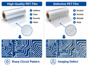
Poor optical transmission or excessive haze can interfere with exposure quality.
Toray’s technical work on polyester film for photoresist explicitly connects film haze with the transparency needed for exposure and notes that excessive haze can result in insufficient exposure and poorer resolution.
For PCB manufacturers, this means PET base film should be evaluated not simply as a clear film, but as an optically controlled process material.
Important questions include:
- Is transmittance consistent across the roll?
- Is haze sufficiently low for the intended imaging process?
- Are there local optical defects?
- Does the film introduce non-uniform exposure?
These considerations become even more important as circuit patterns become finer.
Surface Quality and Fine-Line Resolution
The surface of the PET film directly interfaces with the photosensitive layer.
Excessive surface irregularity can affect coating uniformity and imaging behavior, while an excessively smooth surface can create its own handling and winding challenges.
Toray’s patent work therefore treats surface roughness as a carefully controlled parameter rather than simply maximizing smoothness. It links appropriate roughness to both photoresist performance and film rollability.
Toray’s more recent semiconductor-film presentation also highlights advanced film surface design, industry-leading smoothness, uniform thickness, and control of contamination and scratches for high-end DFR applications.
This is a useful principle for buyers:
the ideal PET base film is not merely transparent—it must have a highly controlled surface.
Controlled Peeling After Exposure
After the photosensitive layer has been exposed, the PET carrier must be removed cleanly.
If the carrier tears, stretches excessively or separates irregularly, it can disrupt the downstream development process.
Toray’s photoresist PET-film patent specifically addresses problems such as film cleavage and elongation during peeling and links film structure and orientation to peel behavior.
This means a good PCB PET carrier needs a careful balance between:
mechanical strength + dimensional stability + controlled peel behavior.
It should be strong enough to withstand processing, but should not create unnecessary stress during removal.
Why PET Film Quality Matters More as PCB Lines Become Finer
Printed circuit boards have continued to move toward finer wiring and higher circuit density.
Toray specifically cites miniaturization of circuit-board wiring and high-end circuit formation as factors increasing the requirements placed on DFR films.
As feature sizes become smaller, defects that were previously tolerable can become much more significant.
Examples include:
- localized haze;
- scratches;
- gels or inclusions;
- thickness variation;
- surface defects;
- wrinkles;
- foreign particles;
- and poor flatness.
A large defect may be obvious during inspection.
The more difficult problem is a small defect that locally changes exposure or coating behavior and later appears as a circuit-pattern defect.
For this reason, PCB-grade PET film manufacturing requires particularly strong control of film forming, surface design, coating compatibility, cleanliness and quality inspection.
https://langyitechglobal.com/solutions/
Key Properties of PET Base Film for DFR
Transparency and Haze
Optical transparency is essential because UV energy must travel through the PET film before reaching the photoresist.
Haze describes light scattering through the film.
In general, lower and more consistent haze supports better optical control, although the exact acceptable value depends on the specific DFR formulation and exposure process.
Toray’s photoresist polyester patent demonstrates that haze must be controlled together with film structure and surface roughness to obtain good photoresist resolution.
Surface Smoothness
Surface smoothness influences:
- coating uniformity;
- contact with the photoresist;
- optical consistency;
- winding behavior;
- and film handling.
General high-transparency PET-film technology also illustrates the importance of particle control, adhesion and flatness. Toyobo, for example, describes high-transparency PET film made without particles in the base layer and emphasizes coating adhesion and superior flatness.
For DFR applications, the required surface profile should be matched to the coating and exposure process rather than assumed from a general packaging-film specification.
Thickness and Thickness Uniformity
PET base film needs enough mechanical integrity for coating, winding and peeling while remaining suitable for high-resolution exposure.
Earlier Toray photoresist-film development specifically addressed relatively thin polyester base films in response to increasing resolution requirements.
The exact thickness should therefore be confirmed with the dry-film manufacturer.
More important than a headline nominal thickness is often uniformity across the web and throughout the roll.
Toray identifies uniform thickness as a value proposition for advanced DFR PET films.
Cleanliness and Defect Control
In high-resolution PCB imaging, contamination can become an imaging defect.
Typical concerns include:
- dust;
- scratches;
- foreign particles;
- gels;
- surface contamination;
- coating defects.
Toray explicitly highlights DFR film quality that is uniform in thickness and free from contamination and scratches.
For customers qualifying PET base film, cleanliness requirements should therefore be discussed explicitly with suppliers.
Flatness and Dimensional Stability
A PET film used in a high-precision coating and exposure process should remain flat and stable.
Poor flatness may contribute to:
- coating non-uniformity;
- winding problems;
- poor contact during imaging;
- wrinkles;
- web-tracking issues.
Toyobo’s high-transparency PET film technology similarly identifies superior flatness as an important characteristic of high-functionality PET film.
Peelability and Roll Handling
A PET carrier must satisfy two apparently competing requirements:
It must remain securely associated with the photoresist during processing, but it must also peel cleanly at the correct stage.
In addition, the film must wind and unwind without generating wrinkles or handling defects.
Toray’s patent development for photoresist films specifically addresses both peel behavior and winding performance.
PCB-Grade PET Base Film vs. General-Purpose PET Film
Not every PET film is suitable for dry film photoresist.
| Requirement | General-Purpose PET Film | PET Base Film for PCB DFR |
|---|---|---|
| Transparency | Application dependent | Critical for exposure |
| Haze control | May be moderate | Closely controlled |
| Surface smoothness | General-purpose level | Controlled for coating and imaging |
| Thickness uniformity | Standard tolerance | High consistency preferred |
| Cleanliness | Depends on market | High cleanliness required |
| Scratch control | Normal industrial requirement | Critical for fine-line imaging |
| Flatness | General requirement | Important for coating/exposure |
| Peel behavior | Often not relevant | Important process requirement |
| Roll quality | Important | Critical for long coating runs |
| Optical defects | May be tolerated | Can affect circuit imaging |
This does not mean that PCB PET film must always have the most extreme specification in every category.
It means the specification needs to be designed around photoresist coating and PCB imaging requirements.
How PET Base Film Is Used in the PCB Dry Film Process
A simplified process is:
1. Photoresist Coating
A photosensitive resin formulation is coated onto the PET carrier film.
2. Drying and Protective Lamination
The coated photoresist is dried and protected with a PE cover film.
3. Roll Production
The dry-film laminate is wound and supplied as a roll.
4. PE Film Removal
Before PCB lamination, the PE protective layer is removed.
5. Lamination to the PCB Substrate
The photosensitive layer is laminated onto the copper-clad board or other circuit substrate.
6. UV Exposure
The circuit pattern is exposed through the PET base film.
7. PET Carrier Removal
After exposure, the PET carrier is peeled away.
8. Development
Unwanted photoresist areas are removed according to the resist process, leaving the required pattern.
Toray describes this basic sequence in its polyester-film technology for photoresist applications.
Common PET Base Film Problems and Their Impact
High Haze
Potential impact: reduced exposure quality or poorer imaging resolution.
Surface Scratches
Potential impact: localized optical or coating defects that may transfer into the imaging process.
Poor Thickness Uniformity
Potential impact: inconsistent coating, handling or exposure behavior.
Wrinkles or Poor Flatness
Potential impact: web-handling issues and imperfect contact during processing.
Foreign Particles or Gels
Potential impact: localized defects in coated photoresist and possible circuit-pattern defects.
Poor Peel Behavior
Potential impact: stretching, tearing or incomplete separation after exposure.
The important point is that PET film quality and dry-film performance should be evaluated as a system, not as independent materials.
How to Select a PET Base Film Supplier
When evaluating PET base film for PCB dry film photoresist, buyers should discuss more than thickness and width.
A practical supplier-qualification checklist should include:
- Film thickness and tolerance
- Available width
- Optical transmittance
- Haze
- Surface roughness
- Surface treatment
- Coating adhesion
- Flatness
- Dimensional stability
- Cleanliness and defect specification
- Scratch control
- Peel behavior
- Roll length and winding quality
- Slitting capability
- Consistency between production lots
- Experience supplying dry film or electronic-material applications
This last point is especially important.
A supplier with experience in packaging PET film may have excellent manufacturing capability, but PCB dry-film applications require a different level of optical, surface and cleanliness control.
Toray’s film R&D organization specifically identifies dry film resist as a high-functionality polyester-film application requiring dedicated surface and film-processing technology.
PET Base Film Sourcing Support from Hong Kong Langyi
Hong Kong Langyi Technology serves as an international platform connecting global customers with manufacturing and technical resources in China.
For projects involving PET base film for PCB dry film photoresist, supplier qualification should begin with the customer’s actual dry-film process rather than simply requesting a generic PET specification.
Important information may include:
- required thickness;
- film width;
- target haze and transmittance;
- surface-treatment requirement;
- coating chemistry;
- roll length;
- defect limits;
- slitting requirements;
- and annual consumption.
Hong Kong Langyi can help coordinate technical requirements with suitable manufacturing resources within its China supply network. Its official company positioning includes working with selected mainland Chinese manufacturers to provide broader sourcing and supply-chain solutions beyond Langyi’s own product portfolio.
Looking for PET Base Film for PCB Dry Film Photoresist?
If you are manufacturing:
- Dry Film Photoresist
- PCB Imaging Materials
- Fine-Line PCB Materials
- Electronic Functional Films
- Photosensitive Film Laminates
the right PET carrier should be qualified according to your coating process, exposure system, resolution target and roll-processing requirements.
Contact Hong Kong Langyi with your PET base film specification, required thickness, width, optical properties and annual demand. We can help evaluate suitable China manufacturing resources and coordinate sample testing. https://langyitechglobal.com/contact/
Frequently Asked Questions
What is PET base film used for in PCB manufacturing?
PET base film acts as the transparent carrier for the photosensitive resin in dry film photoresist. It supports the resist during coating and handling and remains in place during exposure before being peeled off prior to development.
Why must PET film be transparent in dry film photoresist?
UV exposure passes through the PET carrier to reach the photosensitive resin. Excessive haze or optical defects can interfere with exposure and reduce imaging quality.
Is ordinary packaging PET film suitable for PCB dry film?
Not necessarily. DFR applications place higher emphasis on optical quality, surface control, thickness uniformity, cleanliness, flatness, roll quality and peel behavior. Toray specifically develops high-functionality polyester films for DFR applications.
Why does surface smoothness matter?
The PET surface interacts directly with the photosensitive coating and affects coating uniformity, optical behavior and film handling. Surface roughness must therefore be controlled rather than treated as an incidental property.
Why are scratches and contamination important?
In fine-line PCB imaging, small defects can influence local exposure or coating quality. Toray identifies contamination- and scratch-free quality as an important characteristic of advanced DFR PET film.
What information should I provide when requesting PET base film?
At minimum, provide required thickness, width, roll length, haze/transmittance target, surface treatment, coating requirements, cleanliness or defect limits, application, and estimated annual volume.
External References
- Toray Industries — Polyester Film for Photoresist (JP3932074B2). Describes PET/polyester base-film structure, exposure through the film, peel behavior, haze, surface roughness and winding considerations for dry film photoresist.
- Toray Industries — R&D of Digital Innovation Business. Identifies DFR film as a semiconductor/circuit-board film application and highlights surface design, smoothness, thickness uniformity, cleanliness and scratch control.
- Toray — Film-Related Technical Departments. Lists dry film resist among the company’s high-functionality polyester-film development applications.
- KOLON Industries — Dry Film. Describes dry film as a film material used to form circuits or patterns in PCBs and related applications.
- Toyobo — COSMOSHINE High-Transparency PET Film. Demonstrates high-transparency PET design priorities including coating adhesion and flatness.